Following on from my colleague’s post on using UART to root a phone, I look at another of our challenges, whereby sensitive information such as passwords can be extracted from a device’s memory if physical access to the device is acquired.
The goal and target
The target device is the BroadLink RM Pro universal remote control designed for home convenience and automation.
This smart remote control can be used to control multiple home appliances through its application. It also allows users to create scenarios whereby multiple actions can be programmed and activated simultaneously. Device setup and functionality is accessed through the BroadLink e-Control application. This application must be running on a device connected to the same Wi-Fi network as the smart remote and the appliance you want to control.
For the purpose of this challenge, setting up the device is required. In a real scenario, the device would likely already be set up.
Start by connecting the smart remote to a Wi-Fi network and entering the Wi-Fi SSID and Passphrase within the e-Controls application. The application then subsequently tries to locate the device within the network and once it is found, a connection is established.
Now that the smart remote is functional, an attacker who has physical access to the device may attempt to extract configuration or sensitive information loaded in memory. Successfully replicating this attack scenario is the main goal of this challenge.
Taking a look inside
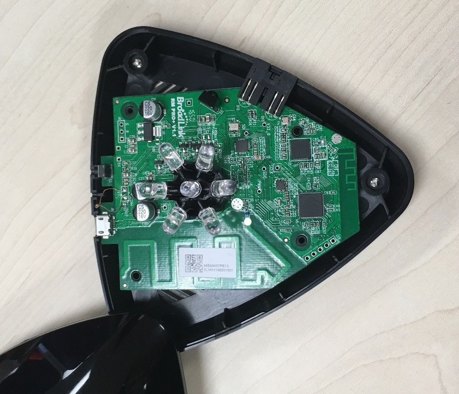
The first step is to investigate the internal components of the device, starting by carefully taking apart the unit. There are three easily removable housing screws situated on the underside of the device.
Once opened, we can then identify different points of interest within the device. These can be internal or external ports, the board’s chips, components, model and serial numbers. Identifying the chip’s model and serial number is essential and will provide us with the information we need in latter stages.
Looking for ways to communicate with the device is another key step. When working with embedded architectures, the presence of debug interfaces such as UART and JTAG is a common method used to establish serial connectivity to the device.
JTAG
Joint Test Action Group or more simply JTAG, is a standardised type of serial communication commonly used by engineers and developers to perform on-board testing or diagnostics of embedded devices, also known as boundary scanning. Another functionality of JTAG, which is seemingly more used today, is CPU level debugging allowing read-write access to registers and memory.
The JTAG interface uses four connection points also known as Test Access Port or TAP. These connection points correspond to four signals:
- TDI – Test Data In; this signal represents input data sent to the device
- TDO – Test Data Out, which represents output data from the device
- TCK – Test Clock, used to synchronise data from the TMS and TDI (rising edge of Test Clock) and TDO (falling edge of Test Clock)
- TMS – Test Mode Select; this signal is used to control the state of the TAP controller
- TRST – Test Reset; this is an optional signal used for resetting the TAP controller
Identifying JTAG pinouts
The implementation of JTAG is non-standardised, which means that the signal pinouts you may encounter will vary between devices. Aside from the standalone JTAG connection points, commonly seen JTAG interfaces may be a part of a 10 pin, 14 pin, 16 or 20 pin header.
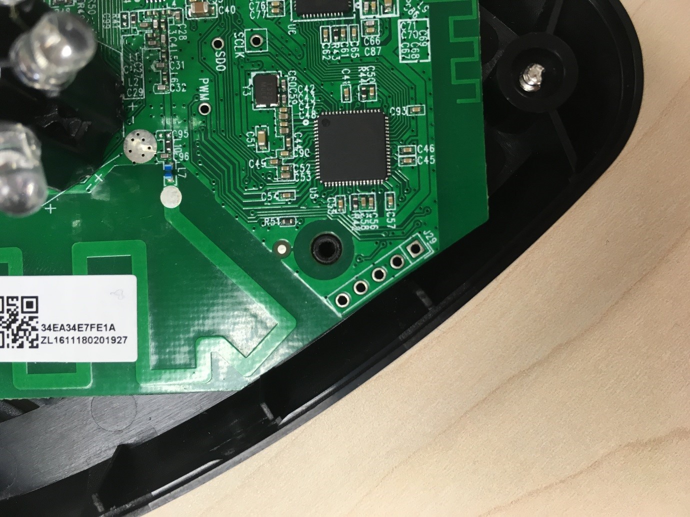
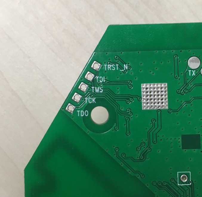
Looking closely at the device, the five connection points on the corner of the board is the JTAG interface. Using the JTAG’s debugging functionality should enable us to read and write data stored in memory.
Note: Some devices will have JTAG present but their connections will have been disabled before being released into production.
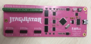
There are various tools available which can be used to identify JTAG signal pinouts, all of which vary in available features and pricing. Common examples are JTAGenum (for Arduino), JTAGulator and Hydrabus to name a few. For the purpose of this challenge, a JTAGulator is used. The JTAGulator supports a number of functionalities, including both the identification of UART and JTAG pinouts.
Connecting the JTAGulator
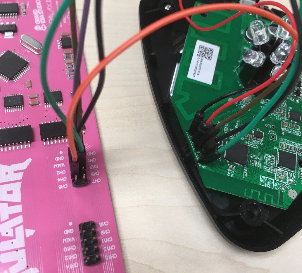
The JTAGulator is connected to the smart remote starting from the lowest number of channels/pins on the board (CH0-CH4). The lowest numbered pinouts are used due to the brute-force method used by the JTAGulator to identify the signal value for each pinout. Using the lowest pin number decreases the number of permutation to iterate through and ultimately speeds up the identification process.
Once connected, you can control using the JTAGulator via USB connection, which will appear as a serial interface. A number of terminal emulators such as PuTTY, Hyperterminal or Minicom can be used to interface with the JTAGulator. In this instance, we will use ‘screen’ utility, which is installed by default on many Linux distributions. It can be used to establish a serial connection to the JTAGulator via the default ttyUSB0 device in Linux machines. The JTAGulator’s baudrate of 115200 should also be provided like so:
$ sudo screen /dev/ttyUSB0 115200
Once a serial connection to the JTAGulator is established, pressing the ‘h’ key shows a list of JTAG commands available. The first step is to set the target voltage to 3.3V, which pertains to the voltage required by the microprocessor. 3.3V is commonly used by most chips; however, accurate information regarding the operational voltage can be found by looking through the chip’s specification sheet. Setting the correct voltage is important as an incorrect voltage could damage or destroy the device. After setting the voltage, the “Identify JTAG pinout (IDCODE Scan) can be used to identify JTAG pins, which works by reading the device IDs – specifically, TDO, TMS and TCK signals. To identify the TDI pin, the BYPASS scan is used.
When running the scans, enter the number of channels to use as five; this will allow the JTAGulator to use the connections made channels CH0 to CH4. The scans should complete fairly quickly as there are only five pins exposed in the board, resulting in a lower number of permutations to be made. If the JTAG implementation appears alongside multiple pinouts, this can increase the number of permutations, thus increasing the duration of the scan.
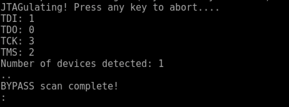
The result of the BYPASS scan show us the location of the signal pinouts on the JTAGulator, which corresponds to the signal pinouts on the smart remote.
You can skip this step entirely if the JTAG pinouts are labelled on the silkscreen print on the board, so do not forget to check both sides of the PCB, as it may save valuable time.
The Shikra
In order for us to get debug access on the smart remote, an interface and some form of OCD (On Chip Debugger) is required. Many devices on the market allow interfacing with JTAG to facilitate on chip debugging, such as Bus Pirate, Shikra and HydraBus. For this scenario, the Shikra and OpenOCD software are used.
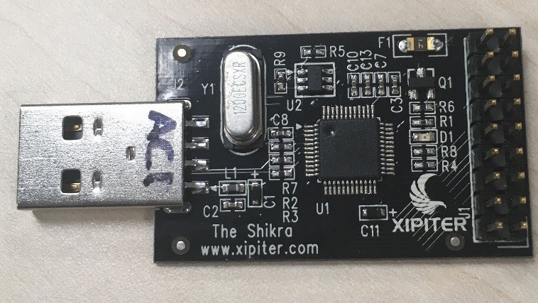
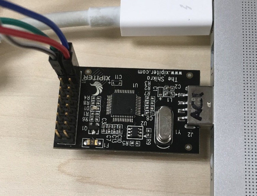
The Shikra is an FT232H USB device sometimes referred to as the “Swiss army knife of hardware hacking”; this device allows us to connect to a number of data interfaces, including UART, JTAG and SPI. A Shikra can be purchased from Xipiter: https://int3.cc/products/the-shikra.
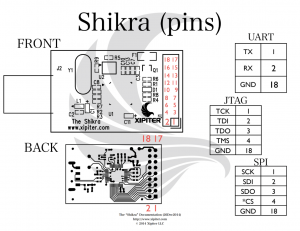
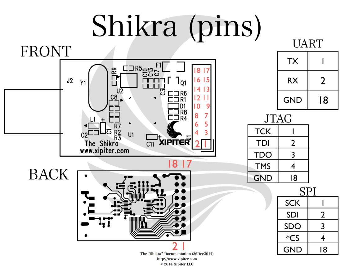
The following diagram shows the Shikra pinouts for JTAG, which will be used to connect to the board’s corresponding JTAG pinouts. Ensure that the ground (GND) pin is also connected to a ground point on the board.
OpenOCD
OpenOCD allows us to perform on-chip debugging of the smart remote via JTAG using GDB. In Linux-based systems, you can install the OpenOCD package by running the following command:
$ sudo apt-get install openocd
In order for us to use OpenOCD, a configuration file for the interface (Shikra) and the target (Smart remote) are required. OpenOCD comes with a number of pre-installed interface and target configuration files; however, the one required does not come in the pre-installed list. The configuration file for the adapter can be found in Xipiter’s getting started guide for the Shikra.
Shikra OpenOCD configuration file:
#shikra.cfg
interface ftdi
ftdi_vid_pid 0x0403 0x6014

ftdi_layout_init 0x0c08 0x0f1b
adapter_khz 2000
#end shikra.cfg
Obtaining the configuration file for the target was not as straight forward. The configuration file required was not available within the pre-installed configuration files and attempting to use any of them results in compatibility errors with the device.
The approach taken in identifying the appropriate target configuration file involved looking up the microprocessor’s make and model. Using a magnifying glass or a good enough camera, the specific chip printings can be determined. The chip in question is a Marvell 88MC200 and a simple Google search of this chip and the keyword OpenOCD returns the target configuration needed.
#
# Marvell's Wireless Microcontroller Platform (88MC200)
#
# https://origin-www.marvell.com/microcontrollers/wi-fi-microcontroller-platform/
#

#source [find interface/ftdi/mc200.cfg]

if " [info exists CHIPNAME] " "
   set  _CHIPNAME $CHIPNAME
" else "
   set  _CHIPNAME mc200
"

set  _ENDIAN little

# Work-area is a space in RAM used for flash programming
# By default use 16kB
if " [info exists WORKAREASIZE] " "
   set  _WORKAREASIZE $WORKAREASIZE
" else "
   set  _WORKAREASIZE 0x4000
"

# JTAG scan chain
if " [info exists CPUTAPID ] " "
   set _CPUTAPID $CPUTAPID
" else "
   set _CPUTAPID 0x4ba00477
"

jtag newtap $_CHIPNAME cpu -irlen 4 -ircapture 0x1 -irmask 0xf -expected-id $_CPUTAPID

set _TARGETNAME $_CHIPNAME.cpu
target create $_TARGETNAME cortex_m -endian $_ENDIAN -chain-position $_TARGETNAME
$_TARGETNAME configure -work-area-phys 0x2001C000 -work-area-size $_WORKAREASIZE -work-area-backup 0

# Flash bank
set _FLASHNAME $_CHIPNAME.flash
flash bank $_FLASHNAME mrvlqspi 0x0 0 0 0 $_TARGETNAME 0x46010000

# JTAG speed should be <= F_CPU/6. F_CPU after reset is 32MHz
# so use F_JTAG = 3MHz
adapter_khz 3000
adapter_nsrst_delay 100
if "[using_jtag]" "
 jtag_ntrst_delay 100
"

if "![using_hla]" "
   # if srst is not fitted use SYSRESETREQ to
   # perform a soft reset
   cortex_m reset_config sysresetreq
"
The above configuration file was pointing to an interface path (line 7) which in our case was not required and therefore has been commented out. The interface configuration file previously downloaded will be used instead and the file location specified as a command line argument in OpenOCD.
Once both target and interface configuration files are saved locally, run the following OpenOCD command:
$ openocd -f /usr/share/openocd/scripts/interface/shikra.cfg -f /usr/share/openocd/scripts/target/mc200.cfg
The file path points to shikra.cfg file, which contains the interface configuration and mc200.cfg contains the target board configuration.
The on-chip debugger should now be running as a server and will open local port 4444 on your system. You can then simply connect to this port with Telnet:
$ telnet localhost 4444
Dumping the device memory
Once connected, debug access to the board is now possible and allows control of registers and memory address.
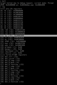
Before the registers can be accessed, sending a halt request is required to send the target into a debugging state. After sending the halt request, the reg command is used to view all of the available registers and its values on the device’s CPU. The full list of useful commands is available in the OpenOCD documentation.
Highlighted in the above image is the Stack Pointer (SP) register. Discussing how computer addressing works is beyond the scope of this blog (it is not a simple subject!). For now, it is enough to understand that the location of the Stack Pointer contains the last value pushed onto the stack of things in memory (RAM), serving as the starting address from where user space memory can be accessed.
Going back to the original goal of extracting sensitive information from the device, the “dump_image” command can be used to dump memory content (in hex). To successfully dump as much information as possible, a trial and error approach to identify the boundaries of user space memory can be taken.
The dump_image command can be used as follows:
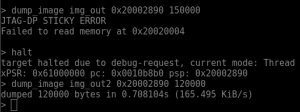
$ dump_image img_out2 0x20002898 120000
The img_out2 argument is the output filename; the next argument is the Stack Pointer address and finally the amount of memory to dump in bytes.
The image above shows that initial attempts at dumping memory may fail if a larger amount of bytes than what is available is specified.
After successfully dumping the contents of memory in hex, an analysis of the file can be performed to identify any information that might be of interest.
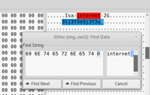
A hex editor of your choice can be used to navigate around the contents of the file and in the example above, we have used Ghex. Looking around the file and by performing a quick search, we can see the SSID name the device is connected to. 18 bytes after it, the passphrase was also shown.
If we had purchased this device second-hand, then we could potentially use it to access someone’s home network and launch further attacks.
Conclusion
Cyber attacks on smart home devices should now be recognised by home consumers, as well as the risks posed should these devices be sold or stolen. On the other hand, manufacturers should consider methods for securing the hardware aspect – the very foundation of these devices – to ensure the security and privacy of its users.
Cisco’s hardware hacking challenges gives us the opportunity to learn different methods to tamper or attack a device, therefore promoting a greater understanding of the security risks and controls they present. This post has presented a simple proof-of-concept attack on a consumer smart device, whereby a user’s Wi-Fi passphrase can be extracted and therefore allow an attacker to achieve persistent access to a victim’s network. This type of attack can be prevented by disabling – or more effectively – removing the JTAG ports completely from production devices, thereby minimising its attack surface.


